

Microstrip Impedance Calculator
Enter Trace Width, Height and Dielectric constant to calculate Microstrip Impedance.
Note: This calculator works for narrow trace(w/h = 1)
Result
- Microstrip ImpedanceOhm
What is Microstrip Impedance?
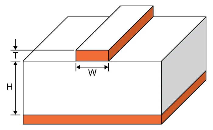
Microstrip impedance refers to the characteristic impedance (Z₀) of a microstrip transmission line formed on a printed circuit board (PCB). A microstrip line consists of a conductive trace on the top layer of a PCB, a dielectric substrate, and a ground plane located underneath the substrate. This structure behaves as a transmission line that carries high-frequency electrical signals.
Characteristic impedance is a fundamental electrical property that determines how signals propagate along the transmission line. It represents the ratio of voltage to current for a traveling wave along the trace and is measured in ohms (Ω). In high-frequency and high-speed electronic circuits, maintaining a controlled impedance is critical to ensure that signals travel through the PCB without distortion, reflection, or excessive losses.
Microstrip transmission lines are widely used in RF circuits, microwave systems, high-speed digital electronics, communication devices, and electromagnetic compatibility (EMC) sensitive systems. Because signals propagate at high frequencies, the physical geometry of the trace—including its width, height above the ground plane, and the dielectric constant of the substrate—directly influences the impedance.
When the impedance of the transmission line matches the impedance of connected components (such as amplifiers, antennas, or connectors), the signal transfers efficiently with minimal reflection. However, if the impedance is mismatched, reflections occur along the trace, causing signal degradation, noise, EMI generation, and performance loss.
Therefore, engineers must carefully design PCB traces with a precisely controlled impedance, commonly 50 Ω or 75 Ω, depending on the application. A Microstrip Impedance Calculator helps determine the required trace dimensions to achieve the desired impedance value.
Uses of Microstrip Impedance
Microstrip impedance calculations are essential in modern electronic design, especially in systems that operate at high frequencies or high data rates. Engineers rely on these calculations to ensure signal integrity and efficient system performance.
Some of the primary uses include:
Controlled Impedance PCB Design
RF and Microwave Circuit Design
Signal Integrity Optimization
Power Transfer Efficiency
High-Speed Communication Systems
Microstrip Impedance Calculation
Microstrip impedance is determined by the physical structure of the PCB trace and the properties of the dielectric material. The most important parameters used in the calculation include:
- Trace Width (w): The width of the copper trace on the PCB.
- Substrate Height (h): The distance between the trace and the ground plane.
- Dielectric Constant (εr): A property of the PCB material that affects signal propagation speed.
- Characteristic Impedance (Z₀): The impedance of the transmission line.
By adjusting the trace width or the substrate thickness, engineers can achieve the desired impedance value for their circuit design.
Microstrip Impedance Equation:
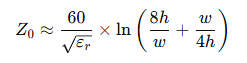
Where:
- Z₀ = Characteristic impedance (ohms)
- εr = Relative dielectric constant of the substrate
- h = Height of the dielectric substrate (distance between trace and ground plane)
- w = Trace width
- ln = Natural logarithm
This equation helps designers determine how changes in trace width or substrate height affect the impedance. PCB design tools and impedance calculators automate this calculation to help engineers quickly determine optimal trace dimensions.
Applications in Electromagnetic Compatibility (EMC)
Microstrip impedance plays a crucial role in electromagnetic compatibility (EMC) design. Poor impedance control can cause signal reflections, which may generate unwanted electromagnetic radiation and interfere with nearby electronic systems.
Properly designed microstrip traces help minimize EMI (Electromagnetic Interference) and improve system reliability.
Reducing Signal Reflections
Minimizing Electromagnetic Radiation
Improving PCB Layout for EMC Compliance
Ensuring Stable High-Frequency Operation
Related Calculators
Other Calculators
- Field Strength Calculator
- Required Amplifier Power for Desired Field Strength
- Amps to dBm Calculator
- Antenna Factor Calculator
- Antenna Near Field & Far Field Distance Calculator
- dBµV/m to V/m Calculator
- Far Field Distance Calculator for Horn Antennas
- Received Field Intensity Calculator
- Received Power Density Calculator
- Required Antenna Gain for Desired Field Strength
Login to EMC Directory to download datasheets, white papers and more content.

Create an account on EMC Directory to get a range of benefits.
 Please wait...